
Research
Wafer-scale CVD growth, van der Waals heterostructures, and catalytic properties of low-dimensional materials.
Programmes
Three research programmes
2D Materials Synthesis & Characterisation
CVD growth of graphene, hBN, TMDCs and halide compounds with controlled layer uniformity for integrated electronics.
Explore →
van der Waals Heterostructures
Stack growth and stacking transfer of wafer-scale van der Waals superlattices and superconductor heterostructures.
Explore →
Interfaces, Catalysis & Devices
Surface adsorption, catalytic properties of low-dimensional materials, and routes toward integrated electronic applications.
Explore →Facilities
Research platforms & equipment
Core platforms that support wafer-scale growth, transfer and characterisation.
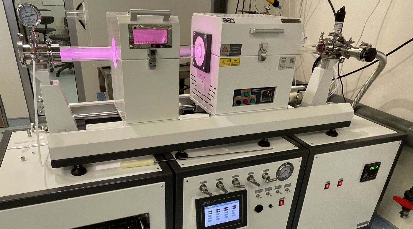
CVD growth
Chemical vapour deposition for graphene, hBN, TMDCs, halide compounds and related 2D crystals.
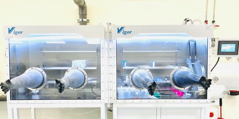
Transfer & stacking
Wafer-scale face-to-face and stacking-transfer routes for graphene films and van der Waals superlattices.
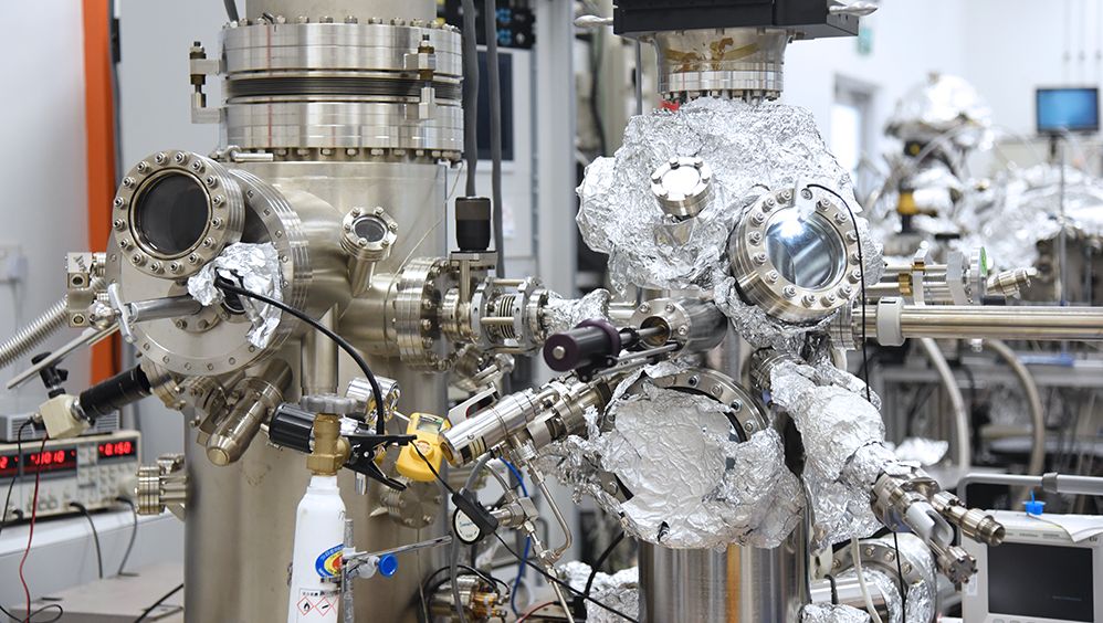
Structural characterisation
Microscopy and spectroscopy used to verify layer uniformity, interfaces and film quality.
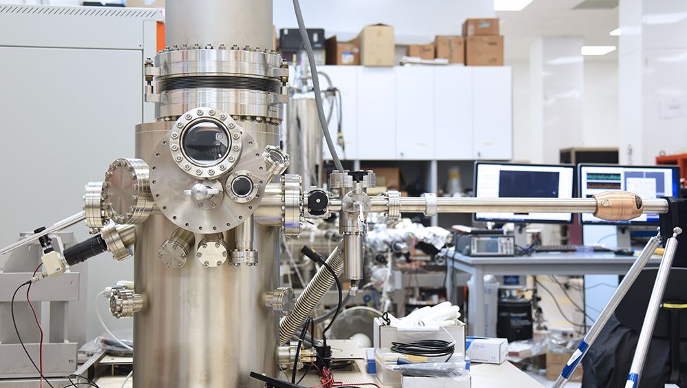
Property measurement
Electrical, optical and catalytic measurements that connect growth quality to device-relevant performance.
Surface & catalysis studies
Adsorption and catalytic behaviour of low-dimensional materials, including proton-related chemistry.
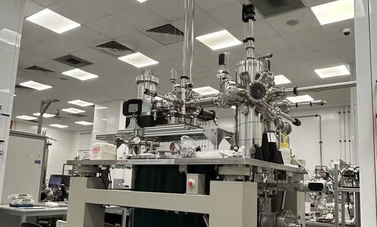
Shared university facilities
Electron microscopy and related core facilities available through Hunan University and partner institutes.
Recognition
Selected awards & programmes
Honours that support the group’s work on wafer-scale 2D materials.